
Gain and phase meter for RF signals
AD8302
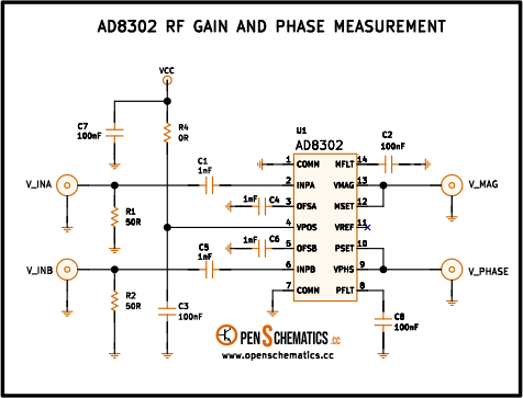
Pinout
| Pin | Function |
|---|---|
| 1 — COMM | Device ground. |
| 2 — INPA | High-impedance input of channel A, designed for AC coupling. |
| 3 — OFSA | Offset compensation terminal for channel A. A capacitor to ground sets the lower corner of the channel. |
| 4 — VPOS | Positive supply, accepted between 2.7 V and 5.5 V. |
| 5 — OFSB | Offset compensation terminal for channel B. A capacitor to ground sets the lower corner of the channel. |
| 6 — INPB | High-impedance input of channel B, designed for AC coupling. |
| 7 — COMM | Second device-ground terminal. |
| 8 — PFLT | Low-pass filter terminal for the phase output. A capacitor to ground sets the detector bandwidth. |
| 9 — VPHS | Output voltage proportional to the phase difference between INPA and INPB. |
| 10 — PSET | Feedback input of the phase-detector loop. Tied to VPHS it sets the default slope and intercept; an external network adjusts them. |
| 11 — VREF | Output of the internal 1.8 V reference. |
| 12 — MSET | Feedback input of the magnitude-detector loop. Tied to VMAG it sets the default slope and intercept; an external network adjusts them. |
| 13 — VMAG | Output voltage proportional to the amplitude ratio (gain in dB) between INPA and INPB. |
| 14 — MFLT | Low-pass filter terminal for the magnitude output. A capacitor to ground sets the detector bandwidth. |
AD8302
The AD8302 is an integrated gain and phase meter for RF signals from Analog Devices. A single chip compares two inputs up to 2.7 GHz and gives back two DC voltages: one proportional to the amplitude ratio in dB and one to the phase difference in degrees.
Both outputs land already in the range of an ADC — 0 to 1.8 V, centred at 900 mV when the two inputs match — with fixed slopes of 30 mV/dB and 10 mV/deg. Each channel covers 60 dB of range, so the gain output spans −30 dB to +30 dB. It replaces the pair of RF detectors and signal-conditioning circuitry that used to be needed to measure amplitude and phase at the same time.
How the circuit works
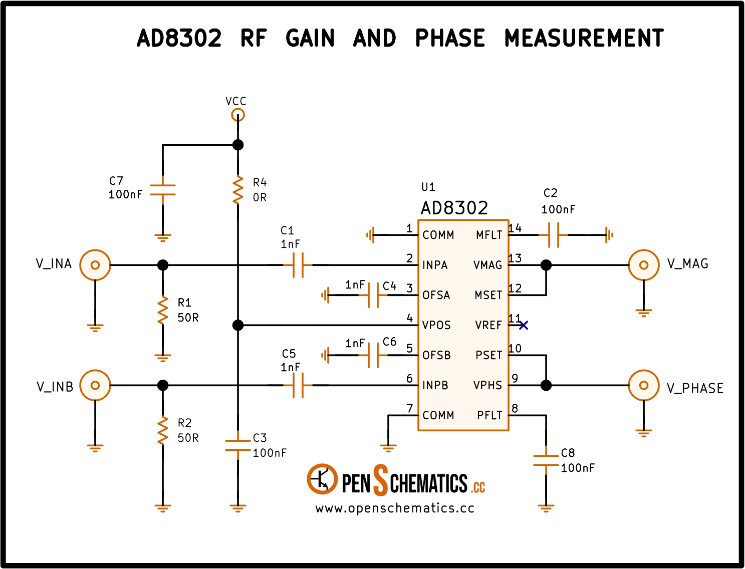
The RF signals come in through the V_INA and V_INB connectors, each terminated to ground by a 50 Ω resistor (R1, R2) that matches the transmission line. The C1 and C5 1 nF capacitors block DC before the INPA and INPB inputs of the AD8302: the chip’s input impedance is high and already set up for AC coupling, so a single series capacitor is enough.
Inside the AD8302, each channel goes through a demodulating logarithmic amplifier that turns the RF level into a voltage proportional to its dB value. The chip subtracts the two logarithmic outputs and puts the result on VMAG (pin 13): the difference of two logarithms is the log of the ratio, so that voltage is directly the gain in dB between the two inputs. In parallel, a detector compares the phases of the two signals and delivers their difference on VPHS (pin 9).
Pins MSET (12) and PSET (10) let you retrim the slope and centre of each output with an external network. In this circuit they are tied directly to their respective outputs (MSET to VMAG, PSET to VPHS): that connection, which Analog Devices calls measurement mode, leaves the chip with its default values — 30 mV/dB centred at 900 mV for magnitude, and 10 mV/deg around the same reference for phase.
Offset compensation and integration. C4 and C6 (1 nF) on OFSA and OFSB set the lower corner of each channel by cancelling the DC offset; C2 and C8 (100 nF) on MFLT and PFLT integrate the magnitude and phase outputs and set the bandwidth of each detector.
Supply and ground. The chip takes VCC on VPOS (pin 4) through a 0 Ω resistor (R4, which acts as a bridge and gives a spot to fit a ferrite if it is needed) and is decoupled with C7 and C3 — 100 nF each — close to the package. The two COMM pins (1 and 7) go to ground. The internal 1.8 V reference on VREF (pin 11) is left unconnected: there is no need to use it because the ADC reading VMAG and VPHS can rely on its own reference, and the chip works just as well with it open.
Application design
The two AD8302 outputs are read as DC voltages. The magnitude one follows the equation:
where is the slope and the centre point, both set by the measurement mode. With both inputs at the same level the log is zero and the output sits at 900 mV; every 10 dB of imbalance shifts it by 300 mV one way or the other, up to the useful range of ±30 dB, where VMAG hits 0 V or 1.8 V.
The phase output responds to:
with and . A phase difference of 90° leaves the output at its centre (900 mV), 0° drives it to 1.8 V and 180° to 0 V, with intermediate values interpolated linearly. The function is symmetric about 0°, so and give the same voltage: the detector does not distinguish the sign of the phase difference. To resolve the ambiguity you add a fixed 90° shift to one of the inputs — with an extra length of line or a phase shifter — so the working phase always sits on one side of the origin, inside the monotonic segment .
Choosing C4 and C6. The lower corner of each channel is , with the internal resistance of the offset loop. With 1 nF, the corner sits around 30 kHz, comfortable from radio frequencies upwards. Going down to MHz just calls for smaller capacitors; extending the response into audio calls for larger ones (10 nF puts the corner near 3 kHz).
Choosing C2 and C8. The internal low-pass filter of each output has an internal resistance of 10 kΩ, so . With 100 nF, the video bandwidth of the output ends up around 160 Hz: enough for a slow ADC and plenty of noise filtered out. Increasing the capacitor smooths the output further — handy if the signal is steady and only the average level matters — and reducing it lets you follow low-frequency modulation, up to the limit of some 30 MHz set by the detector itself.
Supply. The AD8302 accepts 2.7 V to 5.5 V and draws about 25 mA. The 0 Ω resistor R4 and the C7/C3 pair form a standard decoupling network; if the circuit shares its supply with noisy RF stages, replace R4 with a ferrite of a few ohms at 100 MHz.
Other applications
The AD8302 shows up wherever two RF signals need to be reduced to a pair of DC voltages that a microcontroller can read:
- Vector network analysis. Sweep a device with a carrier and measure gain and phase at the same time to obtain the S-parameters in magnitude and angle, the basis of a low-cost scalar/vector network analyser.
- Return loss and VSWR measurement. Comparing the forward signal with the one reflected off a directional coupler, VMAG gives the reflection coefficient in dB and VPHS gives its angle, useful when tuning antennas and filters.
- Automatic antenna and filter tuning. A microcontroller varies the tunable elements while watching VMAG (looking for a minimum reflection) or VPHS (looking for resonance).
- Phase measurement in communication links. Checking phase shifts between I/Q channels or between the two branches of a quadrature stage.
- Phase locking and modulator control. The AD8302 can sit inside a PLL or a vector-modulator loop, providing the error signal proportional to the phase shift between reference and output.
References and further reading
- PDFAD8302 datasheet
This is the main source this article was created from.
- WEB